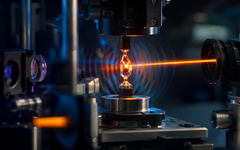
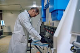
A contract was signed at the Russian forum "Microelectronics 2025" for the supply of the first domestic installation for alignment and projection exposure (photolithographer) with a resolution of 350 nm. The contract was concluded between the Zelenograd Nanotechnology Center (ZNTC) and "Industry Solutions" (part of the Element group of companies).
Today we are laying the foundation for a new stage in the development of domestic microelectronics. The development of an alignment and projection exposure installation with a resolution of 350 nm has been completed at ZNTC, its parameters have been confirmed at the production site, and the transition to mass production is underway. This is the first step in creating a line of Russian lithographers. A serious foundation has been created, which allows us to move on to the development of fully localized installations with 90 nm standards.
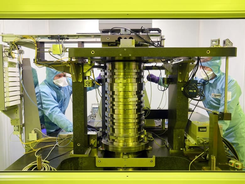
The ZNTC photolithographer is designed for projection transfer of a photomask image onto a semiconductor wafer and its multiplication on the wafer during the manufacture of a very large integrated circuit with a design topological standard of 350 nm. The contract includes the supply, installation and commissioning of equipment.
This installation was created as part of the implementation of one of the first projects of the state program for localizing the technological chain of microcircuit production with topological standards of 350-130 nm. It will be used to modernize existing and equip new microelectronic production facilities. The development and production of the photolithographer were carried out in partnership with the Belarusian OJSC "Planar".
Earlier www1.ru reported that the first photolithographer in Russia with a resolution of 350 nanometers developed in Zelenograd.
Read materials on the topic:
- Breakthrough in optoelectronics: a unique lithographer was developed at MIPT
- A lithographer capable of producing chips at 130 nanometers will be created in Russia
- A new milestone in optoelectronics: a Russian 193-nanometer lithographer may be created in Russia in a couple of years