Zelenograd Nanotechnology Center (ZNTC) has announced the completion of the development of the first Russian photolithographer. This installation is capable of creating microcircuits with a resolution of 350 nanometers.
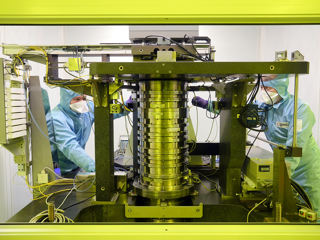
The new lithographer has a number of advantages compared to previous developments. The area of the working field has been increased to 22x22 mm (instead of 3.2x3.2 mm), and the maximum diameter of processed wafers has increased to 200 mm (from 150 mm). For the first time in a Russian lithographer, a solid-state laser, which is more powerful and durable, was used as a radiation source instead of a mercury lamp.
Currently, the center is adapting technological processes to the needs of end users and is negotiating the supply of the first installations for the modernization of existing and equipping new microelectronic production facilities. One of the potential customers is Micron. ZNTC also plans to complete the development of a 130 nm lithographer by 2026.
Earlier www1.ru reported that the first Russian 350 nanometer lithographer went on trial.
Read materials on the topic:
Roselectronica showed the technology for the production of printed circuit boards
Rostelecom is interested in a domestic lithographer and further development of the Aurora OS project
Russia will begin producing printed circuit boards for portable electronics
Комментарии