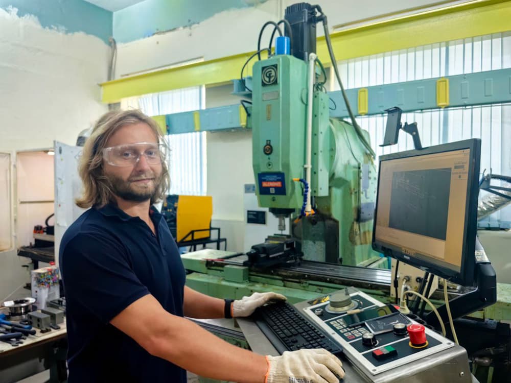
Experts from the Nizhny Novgorod State Technical University named after R. E. Alekseev (NSTU) have created and patented a new software package that optimizes the process of disk cutting of silicon wafers.
The Federal Service for Intellectual Property of Russia issued a certificate of registration for the "Software package for recognizing reference points on silicon wafers in disk cutting units." One of the authors, Dmitry Shakin, said that the complex will increase safety in production, since robots act according to pre-prepared algorithms, which will exclude the possibility of errors.
The process of cutting silicon wafers is extremely important. It is used in areas such as automotive, metalworking, pharmaceuticals, logistics, as well as in the electronic, electrical, food, chemical and glass industries.
The created program is designed to analyze video images from cameras in order to automatically identify reference points on the surface of silicon wafers. It is based on an algorithm that uses methods of binarization, image segmentation, and the Hough transform - a computer vision algorithm for detecting geometric shapes - to accurately determine the coordinates of these points.
According to Shakin, accelerating the work process leads to an increase in production volume, which is achieved through night shifts, work on weekends and the absence of breaks, which ensures uninterrupted operation of equipment.
Read more materials on the topic:
- Engineers from NSTU have come up with a method for accelerated collection and analysis of data at energy facilities
- New software for analyzing brain activity developed at NSTU
- Device for chemical equipment created at NSTU
Комментарии