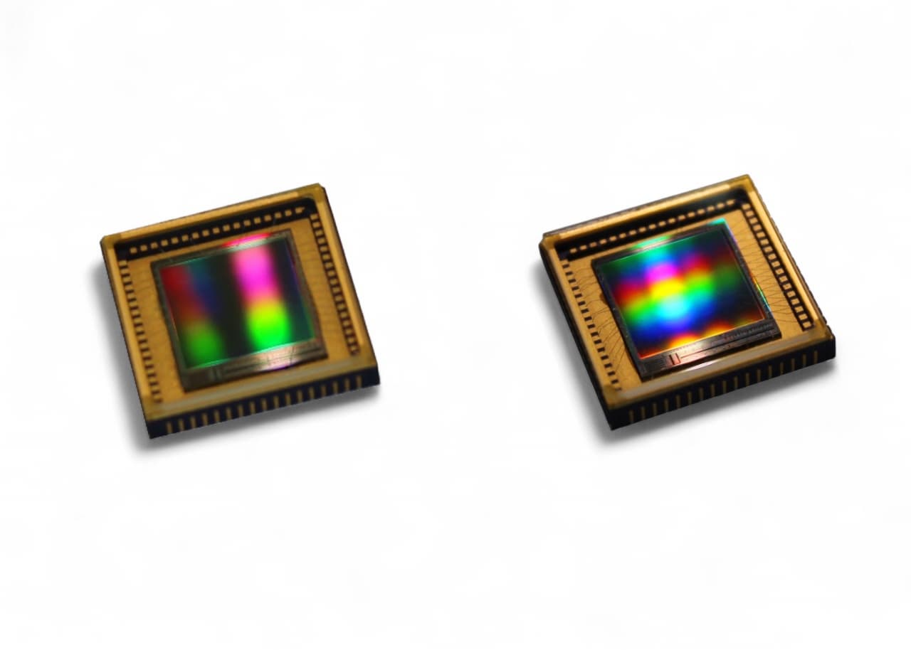
Specialists of the Central Research Institute "Electron" (part of the "Rosel" holding) have developed a new modification of a photosensitive CMOS matrix (complementary metal-oxide-semiconductor structure) with a resolution of 4K. The product is designed for machine vision, video surveillance and industrial automation systems. This was reported in the press service of Rostec.
We see interest from manufacturers of optoelectronic systems who are striving to switch to fully import-independent solutions.
Features of the new CMOS matrix:
- Miniature size
- Energy efficiency
- Analog interface
- Operation at extreme temperatures, vibrations and high humidity
These characteristics were achieved through the use of domestic CMOS technology for building integrated circuits with a 180 nm process.
The main advantage of the CMOS matrix is the integration of the entire image formation system on a single silicon crystal. This reduces the cost of the final technical solution.
The development of the Central Research Institute "Electron" will be useful, including in transport engineering, the oil and gas industry, in the production of medical equipment and industrial sensors. The Rosel holding has launched serial production of highly sensitive matrices.
Read more materials on the topic:
- The first domestic mold compound for protecting microcircuits was tested by Russian engineers
- For accurate processing of X-ray quanta signals: A 16-channel microcircuit was patented at INTEL NRNU MEPhI
- Like clockwork: AI was taught to generate models of digital microcircuits based on a description in Russian
Комментарии