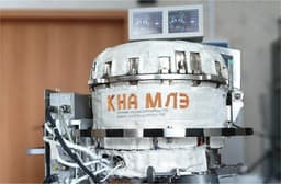
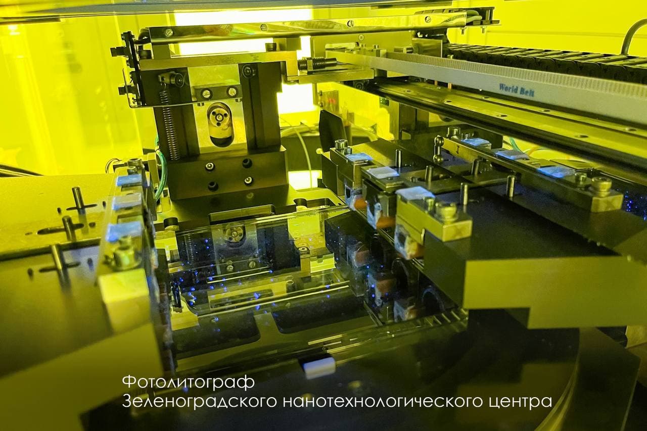
Specialists from the Zelenograd Nanotechnology Center (ZNTC), together with colleagues from Planar (Belarus), have developed the first photolithographer in Russia with a topology of 350 nm. This is a key piece of equipment for the production of microchips, the center's press service reported.

The new joint development has a number of advantages: the area of the working field has been significantly increased - 22x22 mm compared to the previous one - 3.2x3.2 mm, the maximum diameter of the processed wafers is one step larger - 200 mm instead of 150 mm.
Kovalev stated that in other countries, a mercury lamp is used as a radiation source for the production of lithographs. Russian engineers used a solid-state laser, which is characterized by increased power, durability and a narrower spectrum, he added.
ZNTC is also developing an alignment and projection exposure system with a resolution of 130 nm. The work will be completed in 2026.
Read also on the topic:
Going for records: Tutaev Motor Plant produced the 25,000th automotive reduction winch
Import substitution is in full swing: a chip creation facility has been developed at NIITM