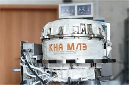
At St. Petersburg Electrotechnical University "LETI" (SPbGETU "LETI"), together with New Diamond Technology, samples of diamond wafers with the addition of boron were created. The development may be useful for power electronics in the near future. This was reported by the press service of the Ministry of Science and Higher Education of the Russian Federation.
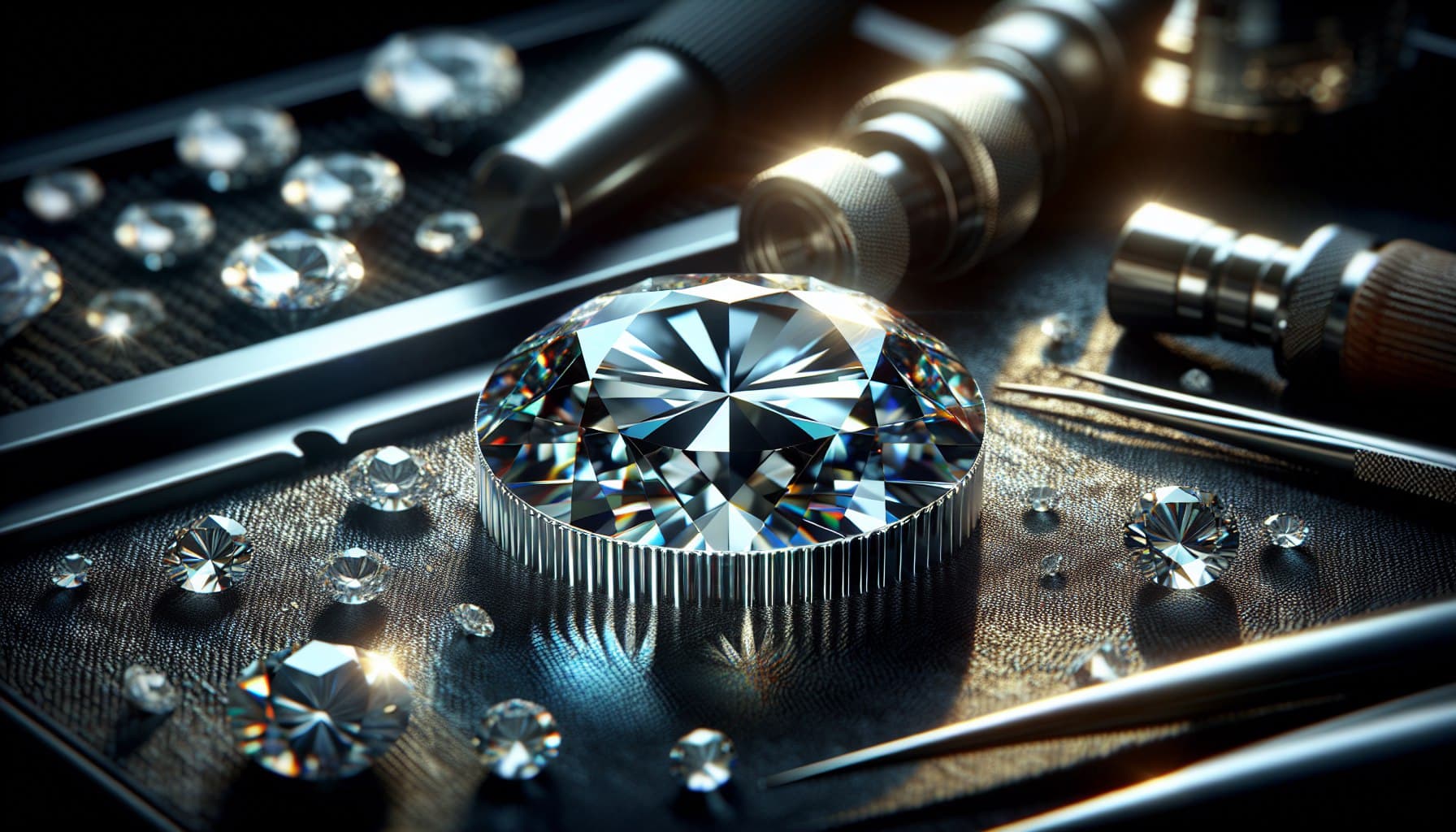
One of the promising materials is synthetic diamond. Of particular interest are diamond crystals with boron impurity, the basis for opto- and microelectronics devices of a new generation.
To create a semiconductor, graphite was placed in a chamber with high pressure (5-6 gigapascals) and a temperature of 1300-1600°C. This made it possible to obtain a diamond crystal in a few days.
At the moment, a sample has been obtained, on the basis of which it is possible to manufacture prototypes of electronic devices. However, for the introduction of developments into mass production, it is necessary to achieve the size of a diamond single-crystal substrate of electronic quality from 2 inches and above with a dislocation density of less than 103 in the minus second degree centimeters.
Earlier www1.ru reported that microcircuits for wireless communication and navigation are being created in SevSU.
Read materials on the topic:
Production of cheap microcircuits in metal-polymer packages launched in Russia
A method for reducing the size of microcircuits has been developed in Russia