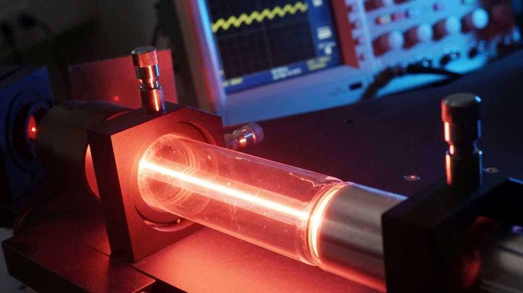
Scientists from the Alferov University, who are part of the consortium of the NTI Competence Center "Photonics", have for the first time in Russia obtained high-quality indium nitride semiconductor crystals on silicon. This promising material can be included in the filling of near-IR photodetectors, gas sensors, devices for transmitting information over long distances via fiber-optic communication lines, quantum telecommunications devices, and photonic integrated circuits.
The main difficulty in the practical application of indium nitride is the high concentration of defects and impurities in the formed crystals. In this regard, it was long believed that this semiconductor has a band gap of about 1.8-2.1 eV, and only in the 2000s, V. Yu. Davydov at the Ioffe Institute showed that the fundamental band gap is about 0.65 eV, and the previous results are due to the low crystalline quality of the samples. In our work, we managed to get closer to the fundamental band gap of this material, which indicates its extremely high quality. The result obtained is a record in Russia.
The Russian solution is more than five times cheaper than its foreign counterparts. The radiation range of indium nitride is about 1.5–2 μm, and the transition to quantum-sized structures, such as quantum dots, will allow creating efficient lasers for transmitting information over fiber-optic communication lines.
Silicon substrates are used for the solution, which cost approximately from $5 per piece. And foreign analogues for creating lasers in the near-IR range from gallium arsenide cost from approximately $80 per piece.
Read materials on the topic:
Hadfield steel has been improved in Russia - it has become even stronger
Russian scientists have created super-strong ceramics using the peel of an exotic fruit
Комментарии