The development of a Russian lithographic machine with a design topological norm of 130 nm is nearing completion. Its acceptance tests are expected to begin this autumn, with completion planned by the end of 2026. This was announced by the head of the Ministry of Industry and Trade, Anton Alikhanov.
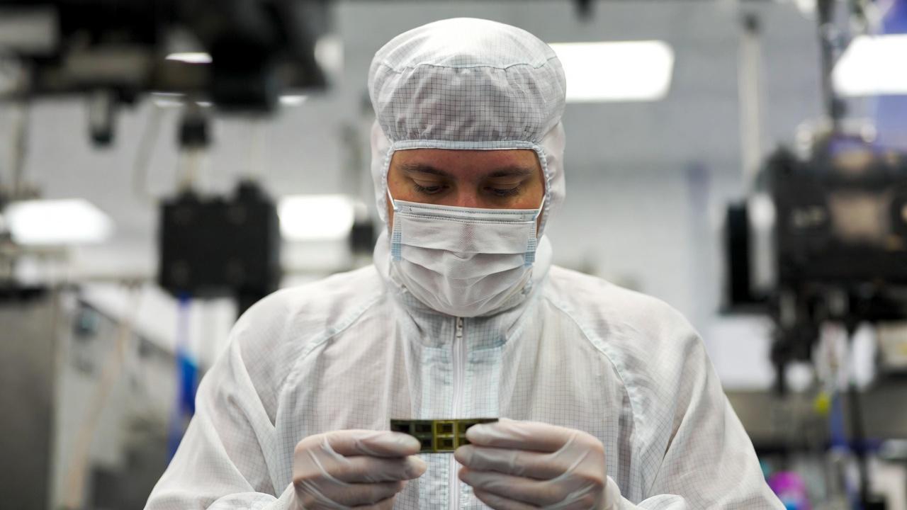
According to the minister, the development of the 130 nm lithographer is “confidently moving towards completion.” Russian excimer lasers, which are the radiation source for such installations, have already passed tests.
Alikhanov also reported that for the next stage, technical specifications for a scanning photolithographer with 90 nm resolution have already been prepared. The selection of the contractor is currently underway.
In August, ZNTC announced the production of a prototype 130-nm photolithographic machine. It is designed to work with semiconductor wafers up to 200 mm in diameter. As part of the project, two prototypes of an excimer laser with a wavelength of 193 nm, photomasks, and test structures were also manufactured.
A lithographer is needed for one of the key stages of microchip production
The machine projects an image of the topological pattern of an integrated circuit onto the surface of a semiconductor wafer. The smaller the topological norm, the smaller the circuit elements that can be formed on the chip.
First, a photosensitive layer — photoresist — is applied to the silicon wafer. Then, the lithographer, like a very precise projector, transfers a reduced image of the microchip pattern from a photomask onto it. After exposure, the photoresist is developed, resulting in the formation of the required pattern on the surface.
According to the resulting pattern, the subsequent operations of the technological process are then performed — for example, etching, ion implantation, or the application of new layers. To form a multilayer structure, these operations and photolithography are repeated multiple times.
The entire wafer is usually not exposed at once. In step-and-repeat machines, the same pattern is sequentially transferred to many areas of the wafer. In scanning systems, the photomask and wafer move synchronously relative to the optical system during exposure.
Read more on the topic:
Never miss our newsAdd this site to your preferred sources to see us more oftenAdd on Google