Russia is taking a new step in microelectronic engineering: in 2027, it is planned to master the production of a completely domestic 130-nanometer lithographer. First Deputy Prime Minister Denis Manturov spoke about the prospects of the industry in an interview with "Kommersant" on the eve of the SPIEF, recalling that last year a 350 nm lithographer was created.
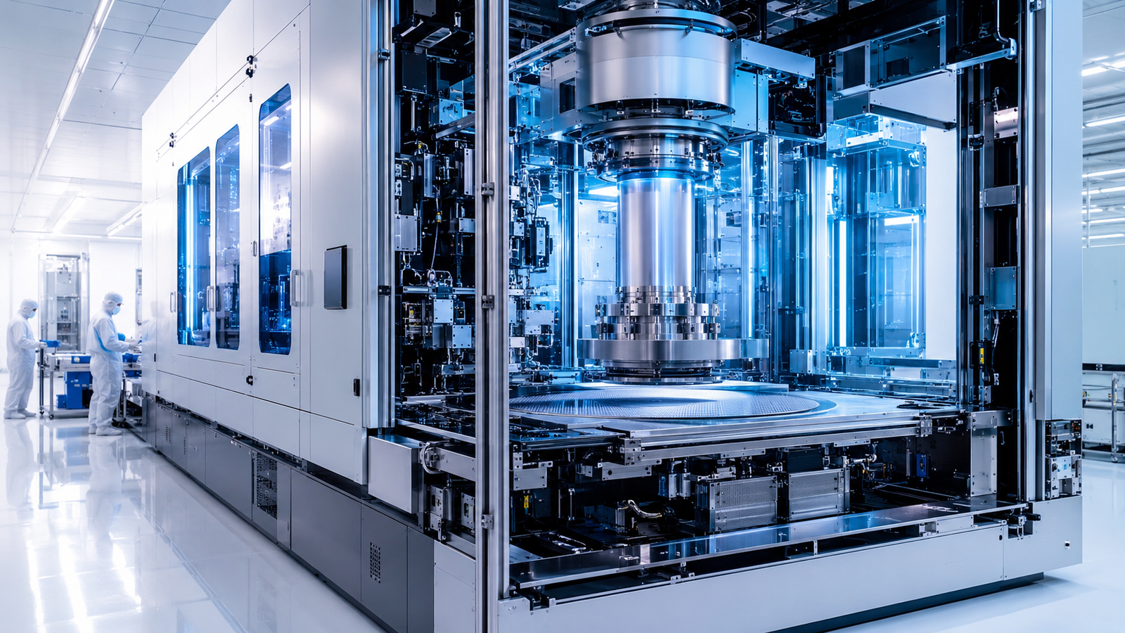
According to the First Deputy Prime Minister, today Russian enterprises serially produce microchips using 300, 200, 130, and 90 nanometer technologies. However, the key task is to develop its own microelectronic engineering, including lithographers and wafer processing equipment, to reduce critical dependence on foreign suppliers, access to which remains limited. The previously released 350-nanometer lithographer became a completely domestic development.
The government is preparing a strategy for a new United Microelectronic Company, which is planned to be approved by the end of the year. The development of microelectronics is considered one of the key areas for achieving technological sovereignty.
What is a lithographer and why is the step to 130 nm important?
A lithographer is a key installation in microchip production that uses light to transfer the pattern of a future circuit onto a silicon wafer. The thinner the technological node, the more transistors can be placed on the chip, which directly affects the performance and energy efficiency of the chip.
A proprietary 130-nanometer lithographer is a transition from a basic level to an industrially significant one: such a topology covers the mass segment of microelectronics, including automotive electronics, industrial controllers, and power electronics. After mastering 350 nm, this is a real step towards technological independence in critical equipment, access to which from outside remains closed.


Комментарии