Zelenograd Nanotechnology Center will develop a Russian scanning electron microscope for microchip production control. The contract, worth 2.37 billion rubles, was concluded with the Ministry of Industry and Trade, and the work must be completed by June 30, 2030.
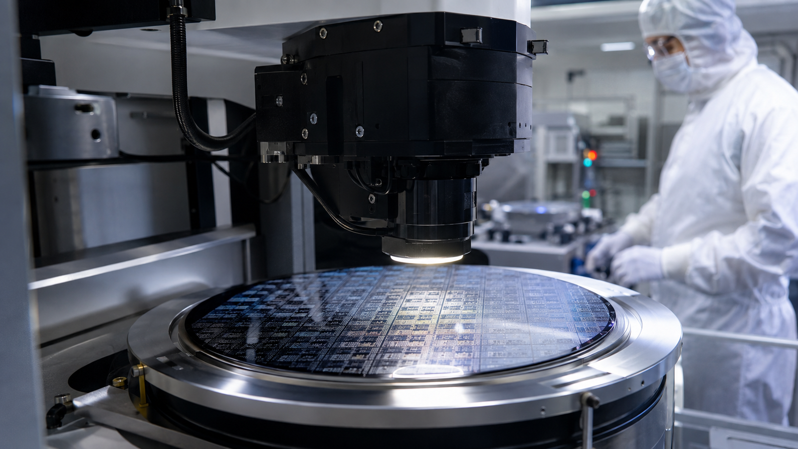
The "Inspector" system will measure critical elements on the surface of silicon wafers: line width, contact hole diameter, distance between structures, and roughness of their edges. The equipment is designed for wafers with diameters of 100, 150, and 200 millimeters, and a prototype will be created for the 200-millimeter format.
Functional analogues are Japanese Hitachi S-9380 and CG4000 microscopes, the supply of which to Russia has been stopped due to sanctions. There are currently no direct domestic analogues of such equipment.
The electron gun, optical column, working chamber, vacuum pumps, wafer loading system, controller, and software must be of Russian production. Imported components will only be allowed after agreement with the customer. The service life of the system must be at least ten years, and the mean time between failures must be at least one thousand hours.
Experts call CD-SEM one of the most complex types of equipment for microelectronics. However, the contract provides for the creation of only a prototype: the transition to mass production will require additional investments, time, and a production base. Earlier, ZNTC already developed a lithographer with a resolution of 350 nanometers and two samples of electron-beam lithography systems for 150 nanometers.
Read more on the topic:
Never miss our newsAdd this site to your preferred sources to see us more oftenAdd on Google