Russian engineers have created an experimental scanning microscope capable of distinguishing details down to 3 nm in size. At the same time, the developers incorporated solutions into the device that allow for research with less impact of the electron beam on the sample.
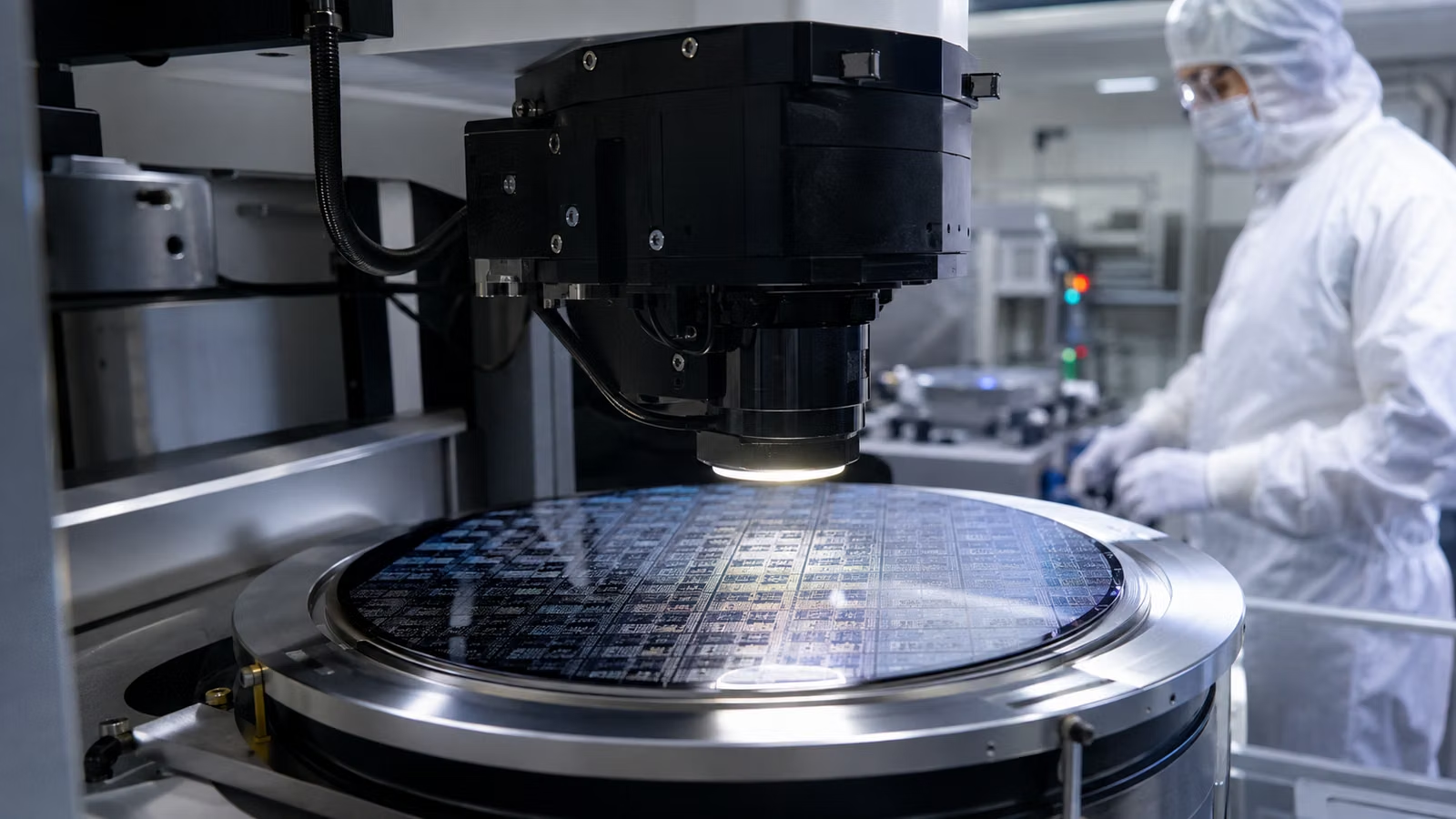
Currently, only an experimental prototype exists, with mass production planned to begin in 2027.
The design provides the ability to choose the cathode material — the electron source. The user will be able to install a more precise and expensive lanthanum cathode or a relatively affordable tungsten one.
Russian engineers also intend to implement a special acceleration system in the production model, which, unlike imported devices, will allow the instrument to operate at lower voltages. This will make it possible to damage materials less during research.
A scanning microscope forms an image by line-by-line scanning of the surface with a focused electron beam. A detector records reflected electrons, after which a computer assembles an image of the sample from the signals.
With a resolution of up to 3 nm, the device can be used for studying alloys and coatings, analyzing microcircuits and chips, as well as examining biological samples.
In the production version, developers expect to bring the share of Russian components to approximately 90%. Thus, for now, we are talking not about ready-made serial equipment, but about an experimental platform on which the technology of the future device is being refined.
Read more on the topic:
Never miss our newsAdd this site to your preferred sources to see us more oftenAdd on Google