Scientists from the Institute of Semiconductor Physics SB RAS and the National Research Center "Kurchatov Institute" have improved a high-k dielectric based on hafnium dioxide. The results of the work can form the basis of non-volatile memory and new generation mobile communications.
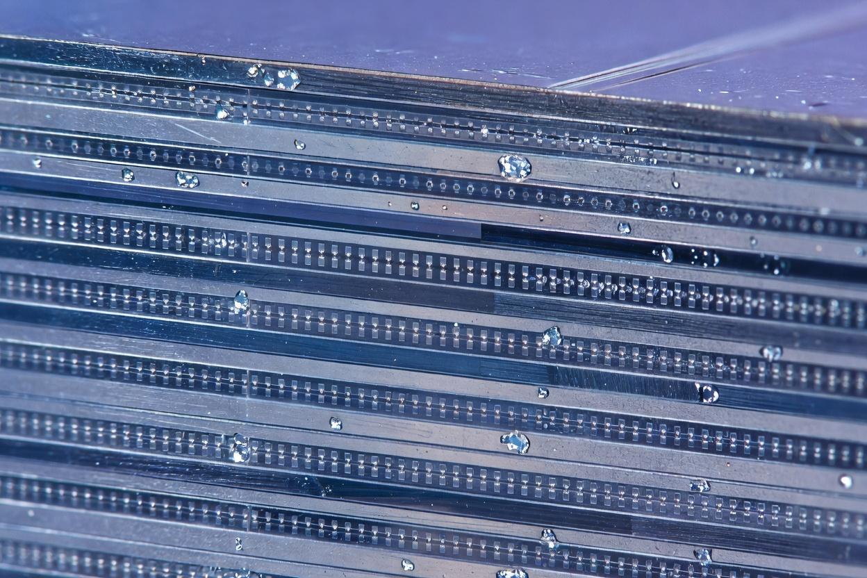
Silicon dioxide is usually used in the gates of transistors in silicon electronics. But there are attempts to replace it with a material with high dielectric permittivity — high-k. One of the candidates is hafnium dioxide.
High-k means high dielectric permittivity. That is, when an electric field is applied, such a dielectric is more strongly polarized and hardly reduces the electric potential. This allows increasing the thickness of the gate dielectric, reducing leakage, and opening the current channel in a field-effect transistor at lower voltages. And, ultimately, creating semiconductor devices with lower supply voltage and power consumption.
Scientists doped hafnium dioxide with aluminum oxide in a 15 to 1 ratio, alternating monolayers of the two dielectrics. The films were grown by plasma-enhanced atomic layer deposition in the laboratory of the K.A. Valiev Department of Physical and Technological Research at the National Research Center "Kurchatov Institute". Then, in the ISP laboratory, they were transferred with a thin layer of silicon onto a silicon substrate.
The research is currently fundamental in nature. Practical application is not yet discussed — only the prospect.
Read more on the topic:
Never miss our newsAdd this site to your preferred sources to see us more oftenAdd on Google