Tomsk scientists have modernized a printer for direct electronics printing: the device applies viscous conductive pastes without stencils and learns to find defects during operation. This was reported by TASS.
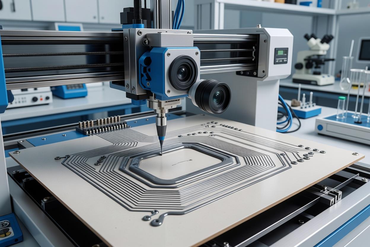
The printer was developed in TUSUR's Additive Printed Electronics Laboratory. The first prototype underwent trial operation in 2024 at a partner's industrial site. The main challenge is multi-layer printing: with a film thickness of about 30 µm, a height difference of 10–15 µm is already critical. A non-contact system is being created to control the distance from the nozzle to the substrate; some solutions are borrowed from a genomic printer.
A video camera was added to the body: the defect recognition algorithm has already been tested on static images. The next step is to adapt it to video streams and refine the dispenser. Direct printing without stencils is especially useful for prototypes and small batches: when changing a pattern, it is enough to change the digital model, rather than manufacturing a new physical stencil.
Read more on the topic:
Never miss our newsAdd this site to your preferred sources to see us more oftenAdd on Google