Translated with AI from the Russian original.
Sberbank has prepared a demand model for Russian microelectronics for the industry – as part of its work on the strategy for the “United Microelectronic Company,” CNews reports. The bank sent it to market participants in mid-August 2026, and at least five companies confirmed receipt.
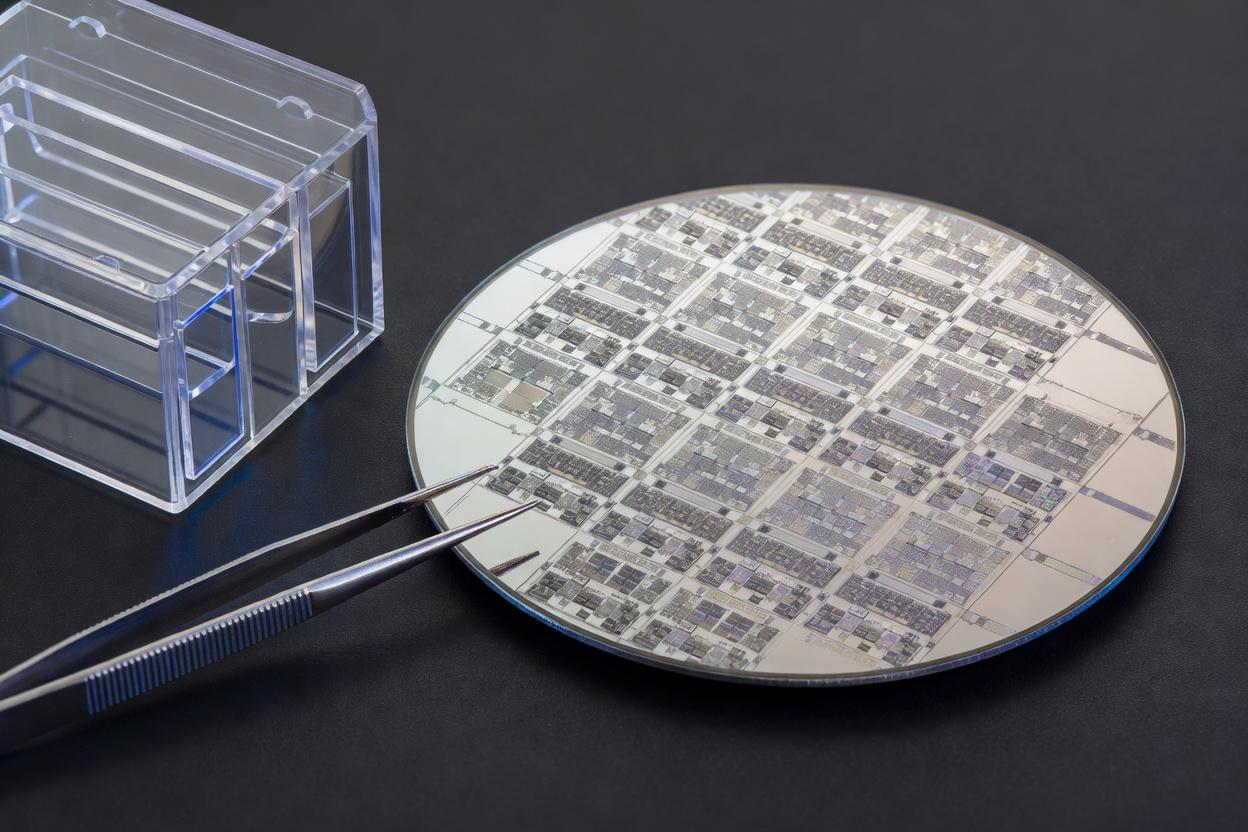
Demand was assessed in two dimensions: by the number of 200 mm diameter wafers and in monetary terms. Such a wafer is a blank from which silicon substrates for chips with topologies from 250 to 90 nm are then cut. In 2025, Russian end products consumed 0.8–1 million such wafers, which corresponds to 500–600 billion rubles in monetary terms.
Three Scenarios
Base scenario: by 2036, demand will double and reach 1.6–1.8 million wafers (1.4–1.5 trillion rubles). By 2030, it will be 1.2–1.4 million. The average annual growth is 7% until 2030, then 5%. This scenario assumes that all approved state programs and investment projects will be fully implemented.
Conservative scenario: growth to 1.1–1.3 million wafers by 2036, i.e., approximately 1.3 times. In 2030 – 1–1.2 million. The average annual growth is 4% and 2% respectively. Here, state programs and investment projects are implemented only by 40%, the focus shifts to B2G, and some projects are postponed.
Optimistic scenario: demand will more than double – to 2.0–2.2 million wafers. In 2030 – 1.3–1.5 million. The average annual growth is 10% and 6%. This assumes full implementation of approved projects plus some additional ones, expansion of regulated demand, and accelerated launch of production.
Where will the growth come from
The main driver is the localization of final products. Out of the total demand growth until 2036, it accounts for approximately 0.6 million wafers. Only an additional 0.2 million comes from the growth of overall demand.
Computational infrastructure and telecommunications consume the most wafers – about 57% of total demand. This includes servers, data storage systems, and network equipment. Industry and transport follow.
Over 60% of demand is formed by memory and logic integrated circuits. However, about 70% of this demand comes from technologies unavailable in Russia – primarily memory and logic at norms less than 16 nm.
Breakdown by norms: 39% of demand is for 45–65 nm, 25% for 90 nm and above, 15% for 28 nm, and only 6% for 16 nm and less. Another 15% accounts for specialized technologies outside classic CMOS.
Industry Assessment
Alexander Timoshenko, head of Troichnye Tekhnologii, drew attention to the technological gap: 70% of demand is for memory and logic less than 16 nm, which are not available in Russia. In his opinion, this gap makes the base growth scenario of up to 1.6–1.8 million wafers by 2036 vulnerable. High stakes and the possible departure of players only exacerbate the problem. Without a breakthrough in its own modern electronic component base, the localization of final products will have a limited effect, so he considers the conservative scenario realistic – unless significant measures are taken.
Read more on the topic:
Never miss our newsAdd this site to your preferred sources to see us more oftenAdd on Google