Translated with AI from the Russian original.
A Russian team led by Evgeny Givargizov, with the support of the National Technology Initiative, has prepared a project for an electron lithograph that should reduce silicon wafer processing from one and a half to two weeks to five to seven minutes. The process will be accelerated by approximately 3000 times by multiple electron beams working simultaneously instead of one.
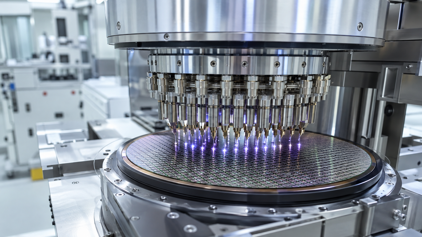
The core of the system is a multicathode — an array of independent electron sources on a common substrate. Foreign systems typically split a single beam with a complex structure of mirrors and gates. The Russian approach should make the equipment cheaper, more economical, and less demanding on infrastructure.
The multicathode technology itself has already been created and tested, but the lithograph currently exists only as a project. The first prototype is planned to be assembled in about three years. Engineers managed to obtain beam sources with a tip radius of 1.5–2 nanometers — developers call this one of the best global results.
The system is expected to be used for manufacturing microchips according to standards from 350 to several nanometers. If successfully implemented, it will be able to accelerate chip production and reduce Russia's dependence on foreign equipment, although the final resolution will also depend on the photoresists used.
Read more on the topic:
Never miss our newsAdd this site to your preferred sources to see us more oftenAdd on Google