The Russian Federal Nuclear Center — All-Russian Research Institute of Experimental Physics (RFYaTs-VNIIEF), known as the birthplace of the first domestic atomic bomb, will develop import-substituted equipment for semiconductor production. The enterprise won a competition held by the Ministry of Industry and Trade, and a contract for R&D under the code name "Dentist" was signed on July 6, 2026, for 992.85 million rubles, according to CNews. The equipment is to be developed by October 30, 2029.
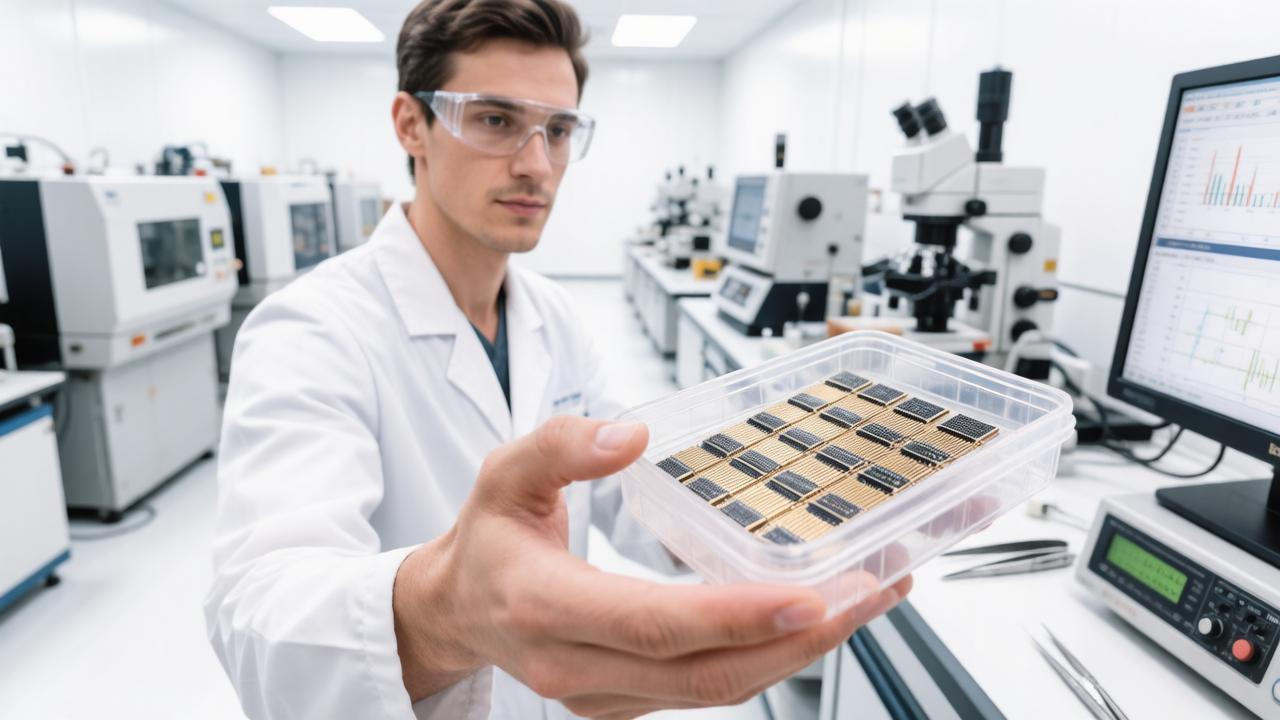
The task involves creating two types of installations: one for temporary bonding of semiconductor wafers with carrier wafers (bonding) and another for their subsequent separation and cleaning (de-bonding). The equipment is designed to work with wafers 100, 150, and 200 mm in diameter.
The new installations are intended to replace Austrian EV Group equipment and German SUSS MicroTec. The key requirement is maximum localization: critically important components, including controllers based on domestic microprocessors, control boards, vacuum systems, and software, must be of Russian production.
The institute was founded in 1946 — it was here that the first Soviet atomic and hydrogen bombs were developed, but today RFYaTs-VNIIEF is actively developing competencies in microelectronics. It includes the Institute of Laser-Physical Research and the Institute of Theoretical and Mathematical Physics. The choice of a nuclear center for such an order is not accidental: the nuclear industry has historically accumulated unique competencies in high-precision mechanics, vacuum technologies, materials science, and complex engineering modeling — these are precisely the skills in demand today in chip production.
Read more on the topic:
Never miss our newsAdd this site to your preferred sources to see us more oftenAdd on Google